Inspection
Microscopic Inspection:
- Particles, scratches, structural defects, vias, bond pads
- Stepper defocusing, homogeneity problems
- Edge Inspection (wafer edce is moged in circular steps along the image field)
- Framed wafer inspektion
- Inspection after sawing the wafer
- Chipping, eruptions, cracks, delamination
Defect Review

Microscopic Review:
- Optical review with defect classification based on imported data of a defect scanning system (e.g. KLARF files)
- Extensive sorting option
- Presentation of imported defect information on a zoomable overview map
- Fast positioning to selected defects even at highest magnification
- Automatic storage of the pictures of the selected defects with several contrast methods and focus levels if necessary
Infrared Microscopy

Infrared Microscopy:
- Transmitted light inspection (through silicon wafer inspection)
- NIR incident light inspection
- NIR polarization microscopy
- Inspection and measurement of buried layers
- Cavity inspection
- Membrane inspection
Thin Film Metrology
Coating thickness measurement for optically transparent layers from 50 nm to 20 µm (coating thickness measurement with spectral refectometry)
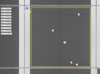
Overlay Measurement

The optical overlay and line width measurement based on light microscopes is a proven non-contact and fast measuring method.
The extreme precision of the measurement results is based on powerful algorithms and the perfectly coordinated combination of microscope, camera and software.
Our MCS system software allows the combination of different tasks like CD and coating thickness measurement or automatic inspection in a mixed process.
Programmed measurement options get reached precisely, new measurement coordinates can be learned quickly by teaching or importing.
Structure Width Measurement / CD
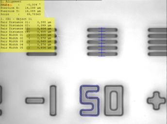
The optical overlay and line width measurement based on light microscopes is a proven non-contact and fast measuring method.
The extreme precision of the measurement results is based on powerful algorithms and the perfectly coordinated combination of microscope, camera and software.
Our MCS system software allows the combination of different tasks like CD and coating thickness measurement or automatic inspection in a mixed process.
Programmed measurement options get reached precisely, new measurement coordinates can be learned quickly by teaching or importing.
The programmed measurement structures were positioned exactly through image alignment. A high-resolution CCD camera records images whose gray value intensity profiles are used for the subpixel algorithms.
The laser autofocus ensures an operator independent and reproducible focusing.
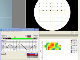
Surface Metrology

Confocal microscope equipment and white light interferometry based on INM200 or DM8000 with hardware & software for topography measurement and export of 3D data. Also available with inspection, CD or thin film measurement.
Typical tasks in quality assurance and research are the characterization of surfaces with different roughness values (wafer structures, mirrors, glass, metals), the determination of step heights and the precise measurement of curved surfaces, e.g. mikro lenses. The efficient, robust and highly accurate evaluation algorithms which are contained in the software are the result of extensive research.
The measurements are based on the interferometry method. This approach is based on the overlapping of spatial and temporal coherent light waves. The beams of the illuminating device are divided by a beam splitter. One part of the light reaches the object surface, the other part gets reflected by a reference mirror. In contrast to many other methods, the image is not scanned pointwise or line by line. The image capturing takes place within seconds (a stack of complete camera frames is drawn in) and the processing of the measuring points is done by the parallel use of many graphics processors (CUDA).
In this way, height information can be obtained over a extensively area in a very short time.
Multisensor Systems flex Wafer
Macro and micro inspection, structural widths, layer thickness and infrared microscopy. Everything on a fully automatic system with flexible robotic wafer handling for batch operation even with different wafer diameters and edge handling if necessary.
Contact us, you will be surprised about the solutions we have realized already.