
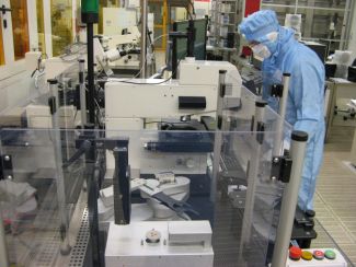
Promicron – Your Partner for Micro-Inspection and Metrology
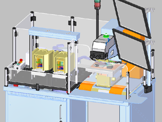
Promicron GmbH stands for innovation, productivity and quality. Based on these principles, we build optical measurement and inspection systems for our customers in the semiconductor industry, that set standards in terms of performance and efficiency. On the base of automatic microscopes, we combine innovative optical technologies with efficient image processing, automatic wafer handling. If desired, we enable a SECS/GEM coupling to our customers MES' production management systems as well. Our in-house programmed software gets steadily driven forward by our highly motivated team.
Wafer Inspection & Measurement
Competences in mechatronics, optics and excellent know-how in software development.
Our engineering and production possibilities allow us to realize sophisticated systems for high-resolution measurement and inspection.
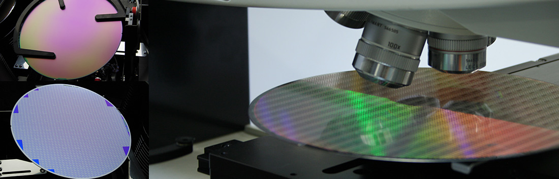
We provide solutions for the semiconductor industry, solar cell production, chip inspection and for the measurement of tiniest structures. Technologies such as white light confocal or infrared microscopy, white light interference as well as wafer front and back inspection: everything is controlled by a modularly constructed MCS software for computer-controlled microscopes.
All engineered solutions – from hardware to software – get customized by 100 percent to your specifications and facilities by our development team.
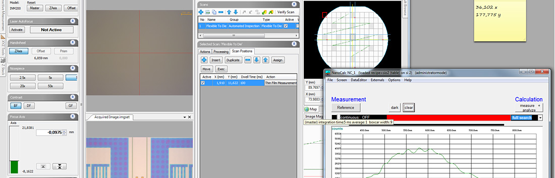
Software Controlled Microscopes
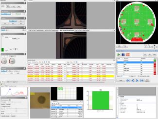
In order to be able to fulfil the high demands of semi and fully automatic inspection and measuring tasks, we provide a modular, standardized software solution: The MCS software suite for documentation and interactive measurement.
The software includes application-oriented modules for research and development as well as for diverse industries, such as the semiconductor industry, the automotive sector, energy and medical technologies. MCS combines automatised microscopes with efficient measurement and contrasting methods. Due to modularity customer-specific adaptations can be made – and it saves your budget at the same time. The integration or update of existing hardware components is also possible.
The software is available in various expansion stages:
- MCS Basic offers pure documentation and measurement functions;
- MCS Standard offers additionally interactive microscope/PC communication for an automatic calibration adaptation;
- MCS Advanced offers further possibilities: automatic control of further hardware such as motorised scanning stages, wafer handling robots, ID readers and much more.
Application Semiconductor Industry
We use the following state-of-the-art techniques for microscopy:
- Interference contrast,
- Dark field,
- i-line UV (365nm),
- DUV (248nm) bright field,
- White-light interferometry,
- Confocal microscopy,
- Focus variation,
- Chromatic height measurement,
- Spectral analyses
For this purpose, there are corresponding software modules for metrology applications available, e.g.: coating thickness measurement, overlay measurement, microscopic optical inspection and review.
We provide specialised tools for many tasks in sectors like structured wafers, bare wafers, masks, solar cells or large-scale substrates, such as OLED.
Setting a special focus on MEMS quality control by AOI and measuring infrared microscopy or rather optical visual inspection according to AQL (acceptance quality level) is very important to us. For this purpose, we use many powerful technologies, such as: LED lighting with triggered image acquisition, image stitching, focus stacking and focus fusion, image alignment, subpixeling and image mosaicing.